| ||||
| Home | EDA Weekly | Companies | Downloads | e-Catalog | IP | Audio | Forums | News | Resources | | ||||
| Check Email | Submit Material | Universities | Books | Events | Advertise | PCBCafe| Subscription | techjobscafe | ItZnewz | RSS | | ||||
| ||||||||
|
|
|
| EDACafe EDA Portal, EDA News, EDA Jobs, EDA Presentations, EDA Newsgroups, Electronic Design Automation. | |||||||||||||||
|
CHAPTER 5
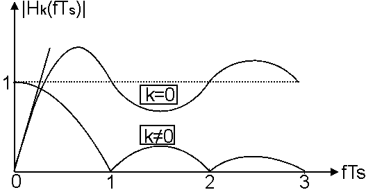
5.2. Ways to reduce offset and 1/f noise Offset and 1/f noise are setting constraints on the obtainable accuracy and dynamic range in the case of CMOS amplifiers. There are several ways to reduce offset and low frequency noise based on sampling or modulation. The autozero technique and correlated double sampling techniques are methods of reducing 1/f noise and offset based on sampling. Due to white noise undersampling, the decrease of 1/f noise and offset is paid by the increase of baseband white noise. In this section the two methods are considered and their advantages and disadvantages are discussed.5.2.1. The autozero technique The autozero technique [2], [3], [4] reduces the offset and low frequency noise based on sampling methods. This method has been extensively used in the past for offset reduction in comparators and amplifiers [4]. Most of the nowadays A/D converters with offset cancellation make use of auto-zeroed comparators. Fig.5.1 illustrates the principle of an autozero amplifier. In the phase 1 of the clock, the sampling phase, the offset and the flicker noise of the amplifier configured as a buffer is sampled on the capacitor C.
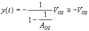
The output y(t) is actually the offset voltage VOS as long as the open loop gain of the amplifier AOL is large:
In the second phase of the clock, the amplification phase, the input signal x(t) is sampled and amplified. The offset and 1/f noise is removed from the output by subtracting the value sampled on the capacitor from its actual output:
The equivalent input offset is reduced by a factor equal to the amplifier open loop gain. The reduction of 1/f noise is based on the high correlation between the 1/f noise samples. The charge injected from the switch produces residual offset which is not cancelled by the autozero mechanism. To show the autozero effect consider a stationary random process n(t) which can be white noise or flicker noise generated by the amplifier A from fig.5.1. For simplicity the amplifier is assumed to have an infinite bandwidth, unity gain A=1 and the input signal is x(t)=0. The equivalent circuit for the noise sampling is shown in fig.5.2. Assuming the switch ideal, the voltage on the capacitor C is an ideal sample and hold signal. If kTs are sampling time instants, h(t) the hold function, the voltage on the capacitor C is:
At the output of the amplifier we have a signal y(t) :
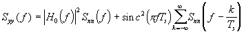
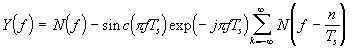
Given the sample and hold of the noise and/or offset on the capacitor C the output spectrum is found to be:
The output noise spectrum is a sequence of spectra shifted at multiples of sampling frequency Ts. The transfer function for every harmonic Hk(f) has a value of:
The transfer function for k=0 has a zero at the origin and acts like a differentiator. Therefore, any DC component of the random process n(t) is cancelled out. That is why this technique is called autozero. Fig.5.3 shows the transfer functions for k=0 and k¹ 0. The power spectral density of the output noise is found from (5.5):
If the random process n(t) is white noise the second term from (5.7) introduces foldover components in the baseband. The first term takes care for 1/f noise and offset reduction. The simple switched current memory cell from Chapter 3 has also autozero properties and therefore flicker noise is reduced. In conclusion, autozero amplifiers will reduce the offset and 1/f noise by using sampling techniques at the expense of increasing the white noise in the baseband. 5.2.2. Correlated double sampling Correlated double sampling (CDS) is another technique for offset and noise reduction [5], [6], [7], [8]. This method has been used in charge coupled devices CCD. The main difference between autozeroing and CDS consists in the way the signal is
delivered to the output. In CDS methods, there are two sampling times. A sampling time for noise only and a second sampling time for noise and signal with opposite sign. In the CDS case the output is a sampled and hold signal whereas for autozeroing, the output is a continuous time output. CDS relies upon the same correlation between 1/f adjacent samples. This method has also the disadvantage of aliasing white noise in the baseband. |
| ||||||||||||||
|
| ||
| Copyright 1994 - 2005, Internet Business
Systems, Inc. 1-888-44-WEB-44 --- Contact us, or visit our other sites: AECCafe DCCCafe TechJobsCafe GISCafe MCADCafe NanoTechCafe PCBCafe | |
| Privacy Policy |

.jpg "Click here for IBSystems")


 (5.1)
(5.1)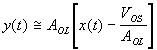 (5.2)
(5.2)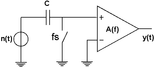
 (5.5)
(5.5)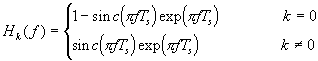 (5.6)
(5.6)